|
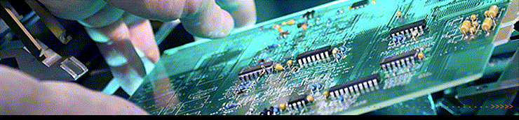
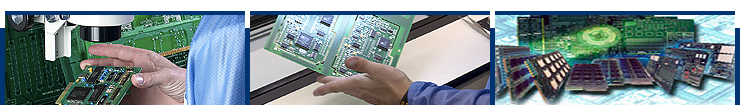
"PSi Technology are the professional PCB Design
service provider. We also provides a full range of PCB design
related products to the electronic industry." We are a highly motivated, dynamic,
engineering-oriented PCB design company. The task of a PCB designer is constantly challenged
by today's evolving semiconductor technological trends and the PCB
manufacturing industry. Our designers are defining creative ways to
deal with semiconductor final product demands as well as meeting the
requirement for the addition of reliability and testing functionality. We offer our quality services at competitive rates;
With a pool of skilled professionals, quick turnaround time and a
commitment to meet your PCB design needs within your specifications.
Whether a simple 2-layer PCB or a complex, high
speed, multi-layer board, our PCB designers can design a board to meet
any performance requirements while minimizing the cost by adopting the
best DFM (Design For manufacturability) rules. Each design is given
special care and attention to ensure a reliable product, while still
meeting your time and board constraints.
By leveraging hundreds of completed designs and an
extensive design and footprint library, we can get the job right the
first time. All designed according to customer specification and
requirements. Internally we are constantly analyzing our design
processes and methodologies to ensure that we can meet our clients
demands for reduced timescales and design complexity.
PSi PCB Design Services is a competent outsourcing
partner for the design of test boards for semiconductor manufacturers
and suppliers.
PCB DESIGN CAPABILITIES
PSi has expertise in board design layout of multi-layer boards. Our
design engineers can handle:
- Designs with Buried & Blind Vias
- Thru Hole and SMT designs.
- Designs with Fine Pitch (0.5mm) sockets.
- Designs with controlled impedance.
- High pin counts (>2000)
- High Speed Digital Design
- Mixed Signal Design
- High Power Board up to 400A/Board
- DFM for best PCB yield from the FAB shop
|
|
PCB TECHNOLOGIES
CAD Tools:
- We use the latest and intelligent CAD tools which minimizes the
design errors and help optimize the routing and part placement.
DESIGN DELIVERABLES
- Design Files
- Net list
- Check plots
- Fabrication drawings
- Assembly drawings
- Gerber files
- Drill files
- Pick and place files
PCB DESIGN OUTSOURCING
FEATURES
- Shortened product design life cycle
- Reduces your design investment on manpower and infrastructure
- Reduced product development cost
- Support of experienced professional for complex designs
- Quick turnaround time
- Guaranteed customer satisfaction
- Disciplined workforce for longtime relationship
|